

(DR)SSTC Nonidealities and Losses
In an ideal world, we'd be able to buy ideal electronic switches on Digikey - such a switch would be able to conduct infinite current with zero voltage across it while closed, hold off infinite voltage with zero leakage while open, switch infinitely quickly while requiring no control power, and be infinitely cheap. Alas, such is not the case, and all of power electronics (and hence all of solid-state coiling) is devoted to circumventing these limitations.
Furthermore, the remainder of the components in a solid-state Tesla coil (the capacitors, coils, and connections) all suffer from parasitics, which, when un-managed, can severely impact the performance of the coil. This article explains these component limitations, and hopefully offers some insight into why solid-state Tesla coils are designed as they are.
Switch Limitations
1. Switch Ratings
Power electronic switches (these days, mostly IGBTs and MOSFETs) have inherent limitations on the voltages they can stand off and the currents they can conduct. The voltage rating on a component is, for all practical purposes, absolute - exceeding this rating will cause instantaneous switch death.
The current rating is much more subtle. Most components these days give a "nameplate" current rating - this is the DC current for which the conduction loss of the switch equals the maximum package dissipation. This assumes no switching, and a constant 25C case temperature - both never true in a practical application.
In reality, maximum allowable current is bounded by two factors. Firstly, the total dissipation must be such that the die never exceeds the maximum allowed temperature (which, for modern devices, is typically 150C, but may be 125C or 175C). This can be computed by a simple thermal analysis.
The other limitation is the safe operating area. This constrains the simultaneous voltage and current that can be present across the switch - a limitation which determines how much current can be safely turned off by the switch. Take, for example, the following diagram:
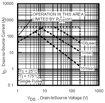
In order for the switch to be able to safely switch a given current at a given voltage, the switching point must be inside the safe operating area. Outside of this area, localized thermal constraints (the die cannot transfer heat to the package quickly enough) or latch-up of the parasitic thyristor structure (in the case of IGBTs) may cause switch failure.
For Tesla coils, which are typically resonant converters, the SOA is rarely relevant, as the voltage being switched is close to zero. However, for the high pulsed currents present in DRSSTCs, localized heating is often an issue - premature failure of IGBTs can often be linked to excessive die heating. The actual temperature of the die during short-pulse operation depends on the mass of the die, which is why nameplate ratings are often non-indicative of DRSSTC reliability.
2. Conduction Loss
The most obvious kind of loss in a switch is conduction loss, which occurs "because the switch is like a resistor when it is on". This is not entirely true. MOSFETs are typically specified by their Rds,on (their "on resistance"); however, Rds,on is varies greatly with current:

From the nameplate current to the maximum rated peak current of 200A, Rds,on increases by over a factor of 2! For a given operating current, the conduction loss of a MOSFET is given by I2Rds,on.
IGBTs, in contrast, behave like diodes. They have a voltage drop which varies logarithmically with current; for small current values, this is often quoted as a "constant" voltage drop; for higher current, this is untrue:
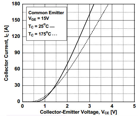
The loss in an IGBT is given by VceI
3. Switching Loss
Switching loss occurs because the current across the switch takes a nonzero amunt of time to rise/fall, and at the same time, the voltage across the switch takes a nonzero amount of time to fall/rise. This results in a condition where the switch briefly has a significant fraction of its standoff voltage across it, and is also conducting a significant fraction of its operating current. The switching loss can be given by k⋅V⋅I⋅tswfsw, where tsw is the switching time, and k is a constant which depends on the shape of the waveforms involved. In general, the best way to get a good estimate of the switching loss in a solid-state Tesla coil is to simulate the design; the complex waveform shapes make an analytical estimate difficult.
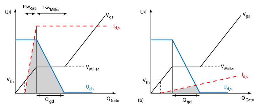
4. Gate Charge
The gate voltage VGE cannot swing between 0 and VG in zero time (leading to switching loss) because of parasitic capacitance CG formed by the gate metal layer, the gate oxide layer, and the body of the transistor. While it is conceptually easy to think of this as a capacitor, in reality, the capacitance is highly nonlinear:

Instead, datasheets typically quote the gate charge, the total charge stored in the gate for a given gate voltage. This value should be used to model switching times for a given gate drive current.
Parasitics
In addition to the inherent limitations of switches, other parasitics play an important part in the operation of a Tesla coil.
1. Parasitic Inductances
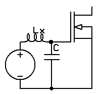
This is perhaps the most important parasitic in a Tesla coil. Because of wiring inductance, there is some inductance in between the DC supply and the switches:
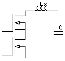
When the switches are on, the inductance Lx carries some current I. When the switch turns off, the inductor current falls roughly linearly; by Faraday's law, this induces a voltage spike across the switch with value given by:

For high switching frequencies and currents, this induced voltage spike can easily lead to switch destruction. It is of paramount importance that the bus inductance Lx be minimized.
In addition, the gate drive circuit, which carries relatively high square-wave peak currents, also contains parasitic inductances:
Similar to in the DC bus, this inductance can ring with the gate capacitance C, causing voltage spikes which are detrimental to the operation of the drive circuit. Depending on the magnitude of the parasitic inductance, this ringing may cause improper switch timings, poor risetimes, or gate oxide failures.
2. ESR and ESL
Real capacitors are not ideal; in applications where high AC currents are flowing through them, they can be lossy. This is due mainly to loss in the dielectric of the capacitor; in a DRSSTC tank circuit, there are hundreds or thousands of amperes flowing through the capacitor, so it is vital that the dielectric be low-loss. Furthermore, the metallization that forms the plates of the capacitor needs to be capable of handling the tank current; typically, this means a foil or hybrid film-foil construction is necessary for larger coils; small coils can get away with standard film capacitors.
The DC bus capacitors are a different story. The ESR of these capacitors is usually in the tens of milliohms - enough to cause significant heating with prolonged operation, but not enough to seriously limit the performance of the coil. However, the ESL of even a small electrolytic capacitor can be tens of nanohenries, and care must be taken to account for this when estimating the parasitic bus inductance.