Step 6: Install the Main Board's Logic Components
| R1 | 4.7Ω (yellow violet gold gold) | |
| C1–C3 | 100uF electrolytic capacitor | |
| C6–C9 | 1uF ceramic capacitor (105) | |
| D1, D2 | 1N4148 signal diode | |
| D3 | Logic-side bridge rectifier | |
| 14-pin socket | ||
| 8-pin socket | ||
| IC2 | Schmitt trigger inverter 74HCT14 | |
| IC3 | LM7815 15V voltage regulator | |
| IC4 | LM7805 5V voltage regulator | |
| IC5 | Dual Gate Driver UCC27425PE4 | |
| Phase jumpers and 2-pin header | ||
| 110V jumper | ||
| Optical receiver | ||
| T1 | Line transformer (110V or 220V) | |
| X1 | 3.96mm 3-pin header |
We’re splitting up the main board assembly process into two steps so that you can clearly see which components are related to the main board’s logic vs. its power. If you wish, you can troubleshoot the main board’s logic after this step to ensure that your construction is correct so far, but you can also install it all at once and troubleshoot the whole system all together later.
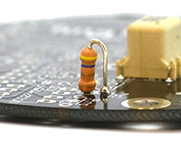
- A. Install R1. Note that it stands on its end (see image below).
 |
Step A: installation of resistor R1. |
- B. Install C1–C3, 100uF electrolytic capacitors. You may need to straighten the leads to have them fit properly. Note the direction! There’s a white band on the negative side, and positive is marked on the board.
- C. Install capacitors C6–C9. They are all 1uF ceramic capacitors labeled 105 whose installation direction do not matter.
- D. Install D1 and D2, the 1N4148 signal diodes. Note that they are directional, and the band on the diode needs to match the band on the board.
- E. Install D3, the logic-side bridge rectifier.
- F. Install sockets for IC2 and IC5. Match the notch on the socket to the notch on the board. Remember, don’t solder the ICs directly to the board!
- G. Insert the ICs into their respective sockets. Remember to match the spot on the IC to the notch on the socket and the board!
- H. Install IC3 and IC4, the 15V and 5V voltage regulators. Don’t confuse the two! They look the same except for the part number.
- I. Install the 2-pin headers labeled JPHASE on the board and slide on the jumpers. The direction of the jumpers doesn’t matter for now.
- J. Install the optical fiber receiver. Be careful! This component is delicate. Soldering this component at too high a temperature can damage it. We recommend soldering at no higher than 400°C. Secure it with a 10mm bolt and M3 nut before soldering it in.
- K. Verify that T1, the line transformer, is rated for the appropriate voltage for your country (110V or 220V). Then solder it in. Please note that the top middle hole is a via that connects the top and the bottom sides of the board, not a hole for a T1 pin.
- L. Install X1, the AC power connector.
Optional Logic Troubleshooting
At this point, you can follow the troubleshooting procedure in step 15 to verify that your work so far is correct. You should first mount your board onto the heat sink.
If you’re confident in your soldering abilities, you can just continue and troubleshoot later if necessary.
Why the pre-soldered component?
The pre-soldered part on your board is a surface mount gate drive transformer (GDT). It’s tricky to solder this component by hand with a regular soldering iron so we did it for you using a heat gun. Through-hole gate drive transformers are bulky, and using this little surface-mount one was the only way we could keep your driver board tiny!

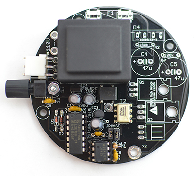
At the end of the step, your board should look like this.

